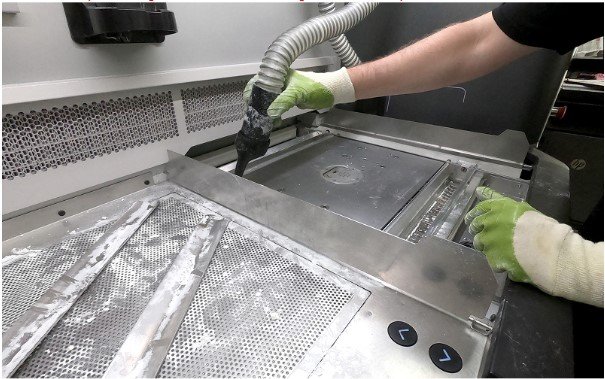
In semiconductor manufacturing, even the smallest contaminant can compromise product integrity. That’s why strict cleaning protocols are essential. From maintaining a controlled environment in a semiconductor clean room to precise semiconductor parts cleaning techniques, the process must leave no room for error. This guide outlines the key procedures that ensure cleanliness, reliability, and operational continuity in semiconductor facilities.
Understand Clean Room Standards and Controls
A semiconductor clean room must be under strictly regulated environmental conditions to operate. The primary goal is to control airborne particles, temperature, humidity, and electrostatic discharge. ISO classifications, ranging from ISO 1 to ISO 9, determine the cleanliness level, with ISO 5 or ISO 6 commonly used in semiconductor environments. Staff must adhere to gowning protocols and enter through air showers to minimise contamination risks.
It’s not enough to build a clean room; continuous maintenance and monitoring are equally critical. HVAC systems with HEPA or ULPA filters must function optimally, while pressure differentials between zones help keep contaminants out. Facilities must also implement particle count monitoring and regular surface wipe tests to ensure compliance with clean room standards. These controls are the foundation for effective semiconductor cleaning operations.
Adopt Proper Semiconductor Parts Cleaning Techniques
Semiconductor parts cleaning involves the removal of particulate, organic, and ionic contaminants from critical components such as wafers, tools, and chamber parts. Cleaning protocols vary depending on the material composition and the type of contamination. Ultrasonic and megasonic cleaning, for instance, are often used for delicate parts. This is due to their ability to dislodge fine particles without damaging surfaces.
Chemical cleaning is another method, especially when targeting specific residues. Acid baths, solvents, and plasma cleaning are selected based on the compatibility with the part and the contamination profile. It’s vital to use deionised water during rinsing stages to prevent ion re-deposition. Effective drying techniques, such as spin-drying or nitrogen blow-off, must follow immediately to avoid watermarks or corrosion. Damage restoration services will know the most suitable method to use depending on what it needs.
Use the Right Equipment and Materials
The cleaning process can only be effective if the proper equipment and materials are utilised. All tools that enter a semiconductor clean room must be clean room-compatible — meaning they don’t shed particles or generate static. Stainless steel, Teflon, and other non-reactive materials are common choices for cleaning tools and containers.
Operators must also use certified clean room wipes, swabs, and approved solvents that meet semiconductor-grade standards. The use of improperly cleaned tools or non-certified chemicals can reintroduce contamination and negate the cleaning process. Regular validation and calibration of cleaning equipment, such as ultrasonic baths and drying systems, ensure reliability in performance.
Implement Operator Training and SOPs
Proper training is critical for staff involved in semiconductor cleaning processes. Operators must understand the specific cleaning methods for different parts and follow standard operating procedures (SOPs) precisely. These SOPs should cover all steps, from pre-clean inspection to post-clean verification.
Mistakes such as cross-contamination, incorrect chemical use, or inadequate rinsing can cause defects in production. Training should include chemical handling, emergency protocols, and equipment operation to reduce risks. Competency assessments and ongoing refresher training ensure that standards are consistently upheld across all shifts and teams.
Maintain Stringent Quality Control and Documentation
Quality control is the final safeguard in any semiconductor cleaning protocol. Each batch of cleaned parts must undergo verification processes, including visual inspection, particle count measurement, and surface analysis techniques such as FTIR or contact angle testing. Traceability is essential, so each part and process must be documented meticulously.
Process validation also includes periodic audits, where cleaning methods are reviewed for effectiveness and compliance. This is important in environments with better standards or new equipment. Facilities that implement robust documentation and quality checks experience fewer production errors and longer equipment lifespans.
Conclusion
Effective semiconductor cleaning goes beyond surface-level procedures. It requires a combination of clean room management, precise parts cleaning techniques, suitable tools, skilled operators, and strong quality control systems. These protocols reduce contamination risks, protect sensitive components, and ensure the reliability of semiconductor production lines.
Need expert support with semiconductor cleaning or restoration? Contact BELFOR Restoration Services for cleanroom-compliant solutions tailored to your facility.


