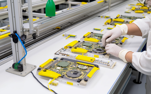
The printed circuit board (PCB) production process begins with translating a customer’s schematic into a physical design layout. PCB board manufacturers in Singapore work with precise CAD software to define trace paths, component locations, and layer configurations. At this stage, layout engineers collaborate closely with clients to ensure the design meets functional, thermal, and manufacturability requirements. Once verified, the design is transferred to production for prototyping.
Prototyping allows the PCB supplier in Singapore to test the feasibility of the design before committing to mass production. It also enables OEMs to validate component placement and performance within the target application.
Preparing Raw Materials for Fabrication
Once the design is finalised, production moves into the fabrication phase. The process starts with copper-clad laminates, which serve as the base material for the board. These laminates are cleaned and prepped to receive the board design through a series of photolithographic steps. Using UV-sensitive films, the PCB manufacturer transfers the circuit pattern onto the laminate with high precision.
Singapore-based suppliers prioritise consistent environmental control during this phase to reduce contamination and variation. The accuracy of this step directly affects conductivity and signal integrity, which are critical in high-speed and high-frequency electronic applications.
Etching and Layering for Circuit Formation
After imaging, the unwanted copper is removed through chemical etching. This leaves behind the desired copper traces that form the electrical paths on the board. For multilayer boards, this process is repeated for each internal layer. These layers are aligned and pressed together under heat and pressure to form a single structure. Via drilling is then performed to connect traces between layers.
A PCB board manufacturer in Singapore must pay close attention to alignment, hole accuracy, and layer bonding strength. Mistakes can compromise electrical performance or board failures later in the field. Quality assurance is embedded in each step to ensure quality before proceeding.
Plating and Solder Mask Application
When the holes are finally drilled, they are plated with copper to have an efficient pathway. The external layers of the board are also plated to enhance durability and conductivity. This is followed by the application of a solder mask, which covers the board surface except where associates will be soldered. The solder mask shields the copper traces from oxidation and helps prevent solder from forming unintended connections.
PCB suppliers in Singapore leverage controlled application methods to ensure precise coverage, contributing to product reliability and aesthetics. Colour consistency, edge definition, and chemical resistance are key criteria in evaluating solder mask quality.
Silkscreen and Surface Finish
After the solder mask, a silkscreen layer is printed onto the board to indicate component labels, logos, and test points. This visual layer supports assembly technicians during the installation of components. The board then receives a surface finish—such as HASL or ENIG—which prepares exposed pads for soldering and ensures long-term solderability.
A PCB supplier in Singapore ensures that the surface finish is chosen according to the board’s end-use environment. Some finishes perform better in high-humidity or corrosive conditions, which are relevant for industrial and medical devices manufactured in the region.
Electrical Testing and Quality Assurance
Before shipment, the finished boards undergo rigorous electrical testing. This step checks for open circuits, short circuits, and impedance irregularities. For complex or high-speed boards, more advanced testing such as automated optical inspection (AOI), X-ray inspection, or flying probe testing may be applied.
PCB providers follow international testing standards to guarantee reliability and consistent performance. Each board must pass inspection before it can proceed to the client or assembly stage. Quality control reports are typically provided to support traceability and compliance documentation.
Packaging and Logistics for Delivery
Final boards are cleaned, vacuum-packed, and labelled for shipment. Packaging standards prevent electrostatic damage or mechanical stress during transit. Singapore’s logistics has fast and secure delivery made possible for manufacturers to meet aggressive schedules and support production models.
Strong logistics support the appeal of partnering with a PCB board manufacturer in Singapore for clients managing short lead times or multiple delivery locations across Southeast Asia.
From design verification to final inspection, the PCB manufacturing process in Singapore is defined by precision, control, and reliability. PCB suppliers in the country combine technical expertise with strong logistics and quality assurance, making them dependable OEM partners.
For more information about PCB supplier solutions in Singapore, contact MPN Tech today.


